STM32H7 (Cortex-M7) GPIO toggling
Introduction
Earlier this year I wrote a post titled micro:bit (nRF51, Cortex-M0) GPIO toggling. Here is a second post on the same concept but this time using a much more powerful ARM Cortex-M7 based STM32H7 series MCU (STM32H723ZG) running at 550 MHz.
The question in this post is as same as before, what is the maximum frequency of a pulse train (square wave) generated just by GPIO toggling, setting an output pin to high and low and repeating this forever ?
Just as a comparison, I will also show pulse trains generated by using DMA instead of a while loop running on the processor, and by using a TIMER.
Since the MCU I am using is clocked at 550MHz, theoretically, assuming writing 1, writing 0, and then looping back each takes 1 cycle, this can be done at 550/3 ~= 183 MHz.
Some of the ideas here are from a thread in STM32 forum.
Setup
All experiments in this post is done with a NUCLEO H723ZG board having an STM32H723ZG MCU. This is I believe one of the most advanced and high performance MCUs in the market. Just to be clear, you should not generate a pulse train by GPIO toggling, this is just an experiment.
I am using STM32CubeIDE and STM32H7 HAL in STM32H7 MCU Package.
The MCU configuration is done in STM32CubeMX inside STM32CubeIDE. After creating the project, I disabled ETH (Ethernet), USART3, USB_OTG_HS and I configured the clock tree to maximum possible, e.g. processor is running at 550MHz, busses are running at 275MHz and 137.5MHz. I enabled PB11 as GPIO Output and set maximum output speed to Very High. Very High here means 220 MHz when used with C=10pF and 100MHz when used with C=50pF (source: STM32H723ZG Datasheet). I also configured Timer 1, Timer 6 and DMA 1 as mentioned in the sections below.
All the measurements are done with a Rohde & Schwarz RTB2004 300 MHz 2.5GS/s oscilloscope using a RT-ZP03 300 Mhz 10:1 probe.
HAL_GPIO_TogglePin
HAL_GPIO_TogglePin with SysTick
The easiest and the most straightforward way to do GPIO Toggling is by using HAL_GPIO_TogglePin in STM32H7 MCU Package. So the code is simply:
while (1)
{
  HAL_GPIO_TogglePin(GPIOB, GPIO_PIN_11);
}
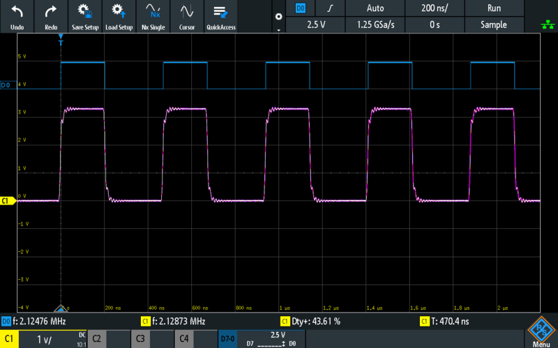
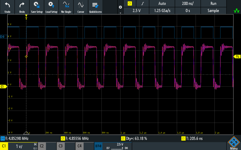
This results:
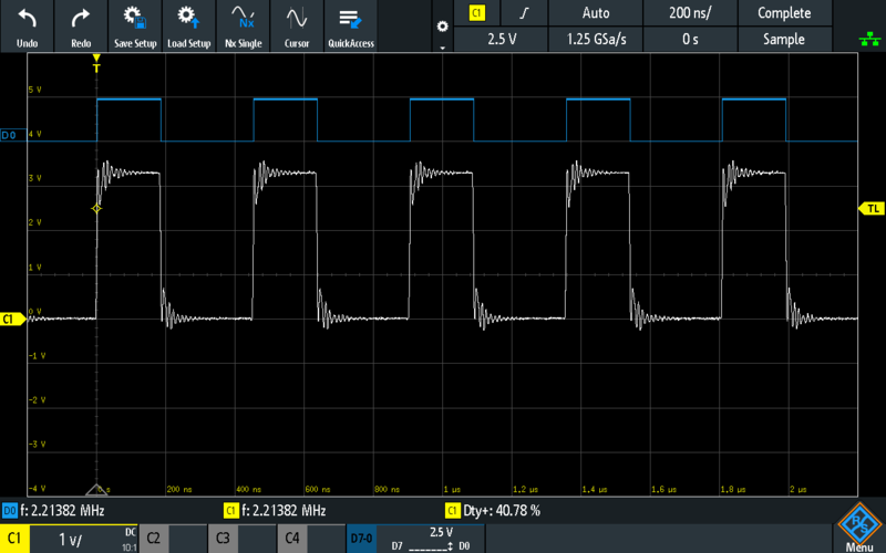
a 2.2MHz pulse train. However, another single trigger can result:
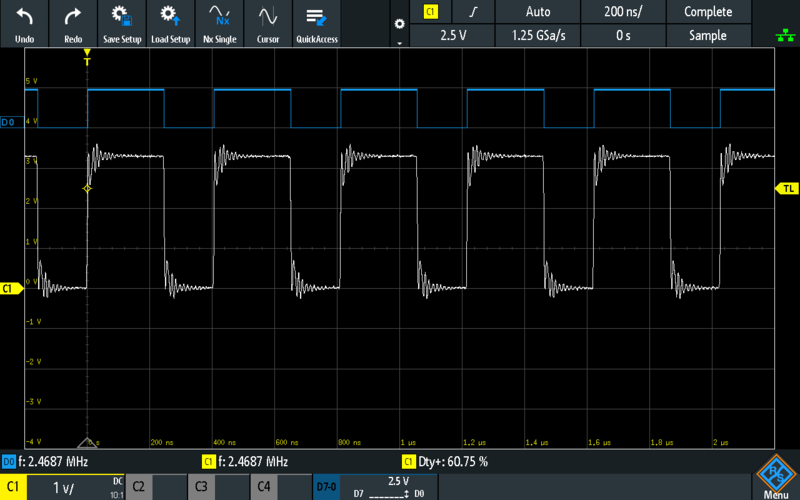
a 2.4MHz pulse train with a different duty cycle. Actually, the oscilloscope shows in continuous mode something like this:
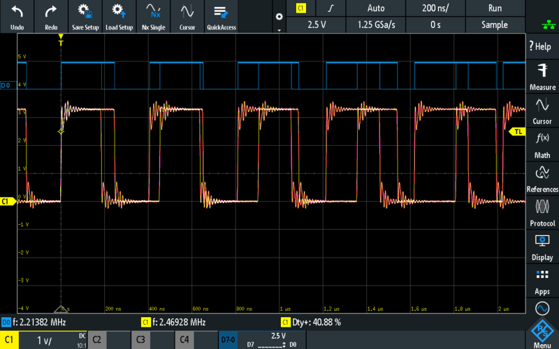
the color is because I selected temperature as waveform color, which shows blue for rare cases and white for frequent ones. This picture does not show everything actually, time to time I also saw other waveforms. So what is going on here ?
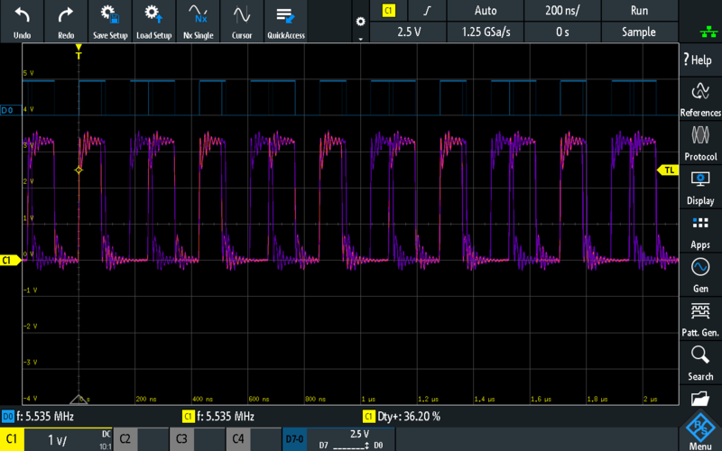
Using history, I could also catch this one:
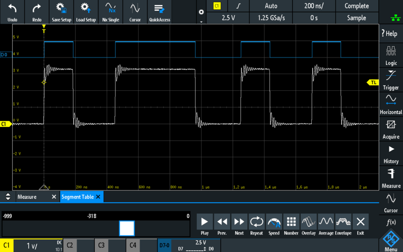
which has an irregular look.
This project, which is just created, has only one thing running concurrently with my TogglePin single line code, which is Systick. Systick timer is a processor feature which generates an interrupt regularly at programmed intervals. The corresponding interrupt handler is called SysTick_Handler and it calls HAL_IncTick which increments a global variable, so it is a short quick running interrupt handler. Depending on where this handler is called, during high or low value of GPIO, that section naturally takes longer than other so duty cycle changes. This also causes the variation in the signal generated by toggling.
SysTick is used by HAL, so normally it should not be disabled, however, for the purpose of this post, it is harmless to disable it and it can simply be disabled by SysTick->CTRL = 0. All experiments below are with SysTick disabled, so you will not see its effect anymore.
HAL_GPIO_TogglePin without SysTick
So the code is now:
SysTick->CTRL = 0;
while (1)
{
  HAL_GPIO_TogglePin(GPIOB, GPIO_PIN_11);
}
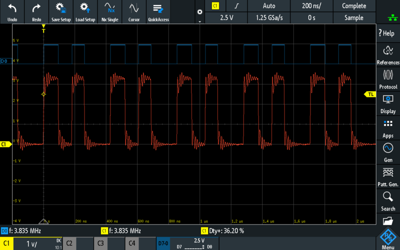
this result the following:
as you see, there is only a single signal, since there is no interrupt, there is nothing causing variation in the behavior of this code.
Also the duty cycle is around 43%, which is close to 50%. You might ask why it is not 50%, it is probably because there is an asymmetric processing done somewhere, I did not check this in detail but we will see an example of this later.
HAL_GPIO_TogglePin with L1 Instruction Cache
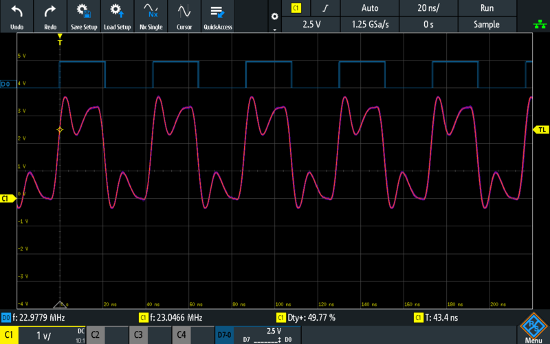
Since Flash memory is slower, there are wait states involved when fetching instructions. So the last thing I wonder is if processor cache changes anything (I expect it should). Cortex-M4 does not have a cache but M7 does, so does STM32H7. So I enabled Instruction Cache (CPU ICache) in STM32CubeMX (which calls SCB_EnableICache() first thing in main) and re-run the code above. The result is interesting:
Quickly single triggering also shows two main signal patterns, which is overlayed also in the above image:
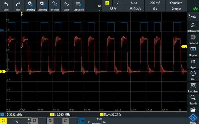
These signals look similar but like shifted or having different duty cycles at each period.
It seems to me this is a signal between 4-5 MHz (one period seems to be a little over 200ns). I think it is fair to say that instruction cache has an effect on the execution above.
Looking at the Disassembly view, the while loop looks like this:
          HAL_GPIO_TogglePin(GPIOB, GPIO_PIN_11);
main+22   mov.w   r1, #2048       ; 0x800
main+26   ldr     r0, [pc, #12]   ; (0x8000334 <main+40>)
main+28   bl      0x8000f0a <HAL_GPIO_TogglePin>
main+32   b.n     0x8000322 <main+22>
and the HAL_GPIO_TogglePin function is like this:
                       HAL_GPIO_TogglePin:
HAL_GPIO_TogglePin+0   push    {r7}
HAL_GPIO_TogglePin+2   sub     sp, #12
HAL_GPIO_TogglePin+4   add     r7, sp, #0
HAL_GPIO_TogglePin+6   str     r0, [r7, #4]
HAL_GPIO_TogglePin+8   mov     r3, r1
...GPIO_TogglePin+10   strh    r3, [r7, #2]
                       if ((GPIOx->ODR & GPIO_Pin) == GPIO_Pin)
...GPIO_TogglePin+12   ldr     r3, [r7, #4]
...GPIO_TogglePin+14   ldr     r2, [r3, #20]
...GPIO_TogglePin+16   ldrh    r3, [r7, #2]
...GPIO_TogglePin+18   ands    r2, r3
...GPIO_TogglePin+20   ldrh    r3, [r7, #2]
...GPIO_TogglePin+22   cmp     r2, r3
...GPIO_TogglePin+24   bne.n   0x8000f2e <HAL_GPIO_TogglePin+36>
                       GPIOx->BSRR = (uint32_t)GPIO_Pin << GPIO_NUMBER;
...GPIO_TogglePin+26   ldrh    r3, [r7, #2]
...GPIO_TogglePin+28   lsls    r2, r3, #16
...GPIO_TogglePin+30   ldr     r3, [r7, #4]
...GPIO_TogglePin+32   str     r2, [r3, #24]
                     }
...GPIO_TogglePin+34   b.n     0x8000f34 <HAL_GPIO_TogglePin+42>
                       GPIOx->BSRR = GPIO_Pin;
...GPIO_TogglePin+36   ldrh    r2, [r7, #2]
...GPIO_TogglePin+38   ldr     r3, [r7, #4]
...GPIO_TogglePin+40   str     r2, [r3, #24]
                     }
...GPIO_TogglePin+42   nop
...GPIO_TogglePin+44   adds    r7, #12
...GPIO_TogglePin+46   mov     sp, r7
...GPIO_TogglePin+48   ldr.w   r7, [sp], #4
...GPIO_TogglePin+52   bx      lr
so one loop has around 25 instructions. Since the processor is running at 550Mhz, assuming all instructions in the while loop takes 1 cycle, there should be 550/4~=140 instructions for each period, which means 2 while loops (one for high, one for low), so there should be like 80 instructions in the while loop, it is not 80 but still close so I think it is a good approximation.
The disassembly above is after a Debug configuration build, but I also created a Speed optimized configuration (Release configuration in the project is optimized for size not for speed) which uses -Ofast option and no Debug information and the result was same so with the Release configuration. I did try the following experiments with different configurations but I only mention if there is a difference, since this is a very simple and low level code, there will probably be no difference.
HAL_GPIO_WritePin
This brings me the next experiment using HAL_GPIO_WritePin instead of HAL_GPIO_TogglePin. The main difference is TogglePin has to read the status of the pin, so WritePin has to be called with a SET and a RESET, and consequently it should have a higher performance.
(I am omitting the SysTick->CTRL=0 part but we have it in all experiments from now on, and also the ICache is enabled)
The code is:
while (1)
{
  HAL_GPIO_WritePin(GPIOB, GPIO_PIN_11, GPIO_PIN_SET);
  HAL_GPIO_WritePin(GPIOB, GPIO_PIN_11, GPIO_PIN_RESET);
}
This results:
which is at 4.8MHz. HAL_GPIO_WritePin method is:
void HAL_GPIO_WritePin(GPIO_TypeDef *GPIOx, uint16_t GPIO_Pin, GPIO_PinState PinState)
{
  /* Check the parameters */
  assert_param(IS_GPIO_PIN(GPIO_Pin));
  assert_param(IS_GPIO_PIN_ACTION(PinState));

  if (PinState != GPIO_PIN_RESET)
  {
    GPIOx->BSRR = GPIO_Pin;
  }
  else
  {
    GPIOx->BSRR = (uint32_t)GPIO_Pin << GPIO_NUMBER;
  }
}
The duty cycle of the signal is 63%, having a shorter low side. The reason for this is pretty obvious because to RESET the signal, the else block runs which does a left shift, so it needs to execute an extra instruction (lsls below). This probably causes the high side to last longer.
                        GPIOx->BSRR = GPIO_Pin;
HAL_GPIO_WritePin+22   ldrh    r2, [r7, #2]
HAL_GPIO_WritePin+24   ldr     r3, [r7, #4]
HAL_GPIO_WritePin+26   str     r2, [r3, #24]
                     }
HAL_GPIO_WritePin+28   b.n     0x8000f0a <HAL_GPIO_WritePin+38>
                         GPIOx->BSRR = (uint32_t)GPIO_Pin << GPIO_NUMBER;
HAL_GPIO_WritePin+30   ldrh    r3, [r7, #2]
HAL_GPIO_WritePin+32   lsls    r2, r3, #16
HAL_GPIO_WritePin+34   ldr     r3, [r7, #4]
HAL_GPIO_WritePin+36   str     r2, [r3, #24]
                     }
GPIO->BSRR
Normal Case
A major change in experiments is to eliminate the HAL function call completely. Since the call basically changes BSRR (Bit Set Reset Register), it can be changed directly, like this:
while (1)
{
  GPIOB->BSRR = (uint32_t) GPIO_PIN_11;
  GPIOB->BSRR = (uint32_t) GPIO_PIN_11 << 16U;
}
this results:
a signal at 23MHz. Naturally, this was a big jump, since function calls are eliminated. Looking at disassembly:
                     	  GPIOB->BSRR = (uint32_t) GPIO_PIN_11;
main+22                ldr     r3, [pc, #20]   ; (0x8000338 <main+44>)
main+24                mov.w   r2, #2048       ; 0x800
main+28                str     r2, [r3, #24]
                     	  GPIOB->BSRR = (uint32_t) GPIO_PIN_11 << 16U;
main+30                ldr     r3, [pc, #12]   ; (0x8000338 <main+44>)
main+32                mov.w   r2, #134217728  ; 0x8000000
main+36                str     r2, [r3, #24]
                     	  GPIOB->BSRR = (uint32_t) GPIO_PIN_11;
main+38                b.n     0x8000322 <main+22>
all code is compacted into 7 instructions (from 25 or so). So the result is not very suprising I guess. The left shift is also optimized at compile time, since GPIO_PIN_11 is known at compile-time.
Optimized Case
How can the code in last experiment be optimized ?
What we need to do is actually to write a memory location (BSRR) once with one value (SET), then with another value (RESET), and then branch to first one.
The code in the last experiment is like this:
[pc + 20] -> r3
0x800 -> r2
r2 -> [r3 + 24]

[pc + 12] -> r3
0x8000000 -> r2
r2 -> [r3 + 24]
The address stored in r3 is GPIOB, pc+20 and pc+12 actually points to the same memory location so what is loaded into r3 is same. 24 is the offset of BSRR, and two values to SET and RESET are loaded to the same register r2. This can be optimized by loading the address of GPIOB->BSRR to a register once, and loading two values to different registers once, instead of loading the registers in the while loop.
This can be done by a c code like this:
register volatile uint32_t* bsrr = (uint32_t*) (GPIOB_BASE + 24);
register const uint32_t set = (uint32_t) GPIO_PIN_11;
register const uint32_t reset = (uint32_t) GPIO_PIN_11 << 16U;

while (1)
{
  *bsrr = set;
  *bsrr = reset;
}
and here is the disassembly of it:
                     	  *bsrr = set;
main+36                str     r6, [r4, #0]
                     	  *bsrr = reset;
main+38                str     r5, [r4, #0]
                     	  *bsrr = set;
main+40                b.n     0x800037c <main+36>
only 3 instructions.
The result is:
like the last experiment, it is 23MHz, so there is no change, and this is interesting, and I will talk a little bit about this later.
DMA
Naturally another way to do the same without using the processor is to use DMA. There are various ways to configure the DMA to have the same effect at the end.
For all the examples below, DMA is configured to transfer data from memory to a peripheral (GPIO) in circular mode increasing the memory address after each transfer. DMA transfer is requested by TIMER 6 (TIM6) having a period of 1, so it should be saturating the DMA unit, since TIMER clock is 275MHz.
DMA without FIFO, from Flash memory
Here is the code:
uint32_t src[2];
src[0] = (uint32_t) GPIO_PIN_11;
src[1] = (uint32_t) GPIO_PIN_11 << 16U;
HAL_TIM_Base_Start(&htim6);
HAL_DMA_Start(&hdma_tim6_up, (uint32_t)&(src[0]), GPIOB_BASE + 24, 2);
__HAL_TIM_ENABLE_DMA(&htim6, TIM_DMA_UPDATE);
src above stays in Flash since it is in the code and the code is kept in the Flash by default. GPIOB_BASE + 24 is the BSRR register. There is nothing else in the while loop, since TIM6, DMA and GPIO works autonomously. This results:
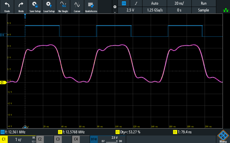
a signal at 12.5MHz. This is less than the maximum before but it is important that src is in Flash memory, and wait states are needed to access the Flash memory.
DMA without FIFO, from SRAM
Moving src to (first 16KB of) SRAM1 which is connected to the bus matrix DMA1 is also connected:
uint32_t* src = (uint32_t*) D2_AHBSRAM1_BASE;
src[0] = (uint32_t) GPIO_PIN_11;
src[1] = (uint32_t) GPIO_PIN_11 << 16U;
HAL_TIM_Base_Start(&htim6);
HAL_DMA_Start(&hdma_tim6_up, (uint32_t)&(src[0]), GPIOB_BASE + 24, 2);
__HAL_TIM_ENABLE_DMA(&htim6, TIM_DMA_UPDATE);
this results:
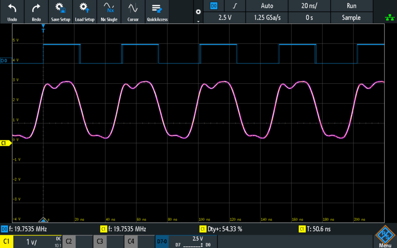
a signal at 19.750MHz.
DMA with FIFO, from SRAM, single transfer
Keeping the code same, FIFO can be enabled which should be useful. Since accessing SRAM is faster than GPIO, FIFO can be filled easily. I configured the DMA to use FIFO with Full Threshold. This results:
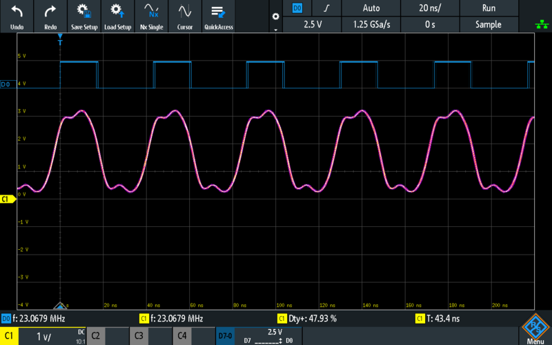
a signal at 23MHz, like the last experiment using the processor.
Lets look at the DMA connections:
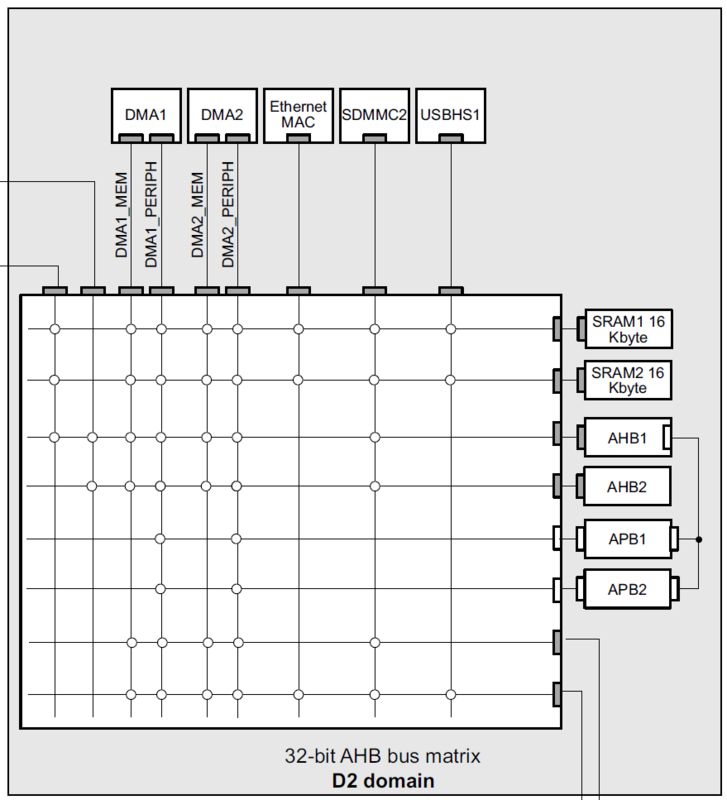
My understanding is, in order for DMA to write to APB2 where GPIO stays, it has to go through AHB2 and then pass AHB-APB bridge, and reach APB2. I am not sure if this calculation is correct:
- DMA arbitration is 1 AHB cycle. 1/275~=3.75ns
- I assume with the use of FIFO, SRAM access is independent so I do not count SRAM read latency.
- AHB-APB bridge is 1 AHB cycle. 1/275~==3.75ns
- APB write is 2 APB cycles. 2/137.5~=1.5ns
In total, 9ns ~ 100 MHz. I think there should be still a way to increase the frequency of the signal by GPIO toggling a bit but I could not find a way yet.
TIMER
Toggling Forced Output
This is not a normal use of a TIMER but it is possible to toggle GPIO pin through a TIMER using the Forced Output mode. I configured TIMER 2 (TIM2) in Forced Output mode and set and reset the forced output active/inactive bits in CCMR1 register.
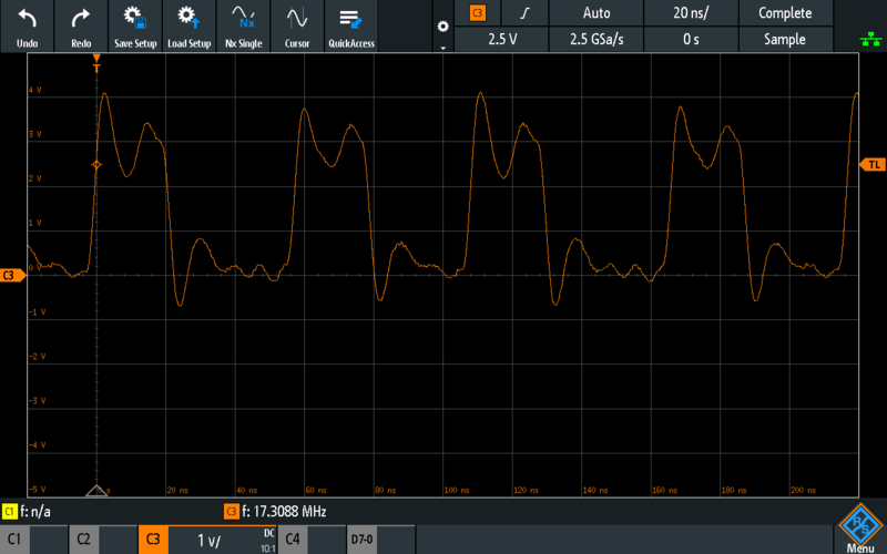
shows a signal at 17Mhz.
PWM Output
The best thing to use to generate such a signal is to use a TIMER. I configured TIMER 1 (TIM1) in PWM mode (period=1, pulse=1), and here is the result:
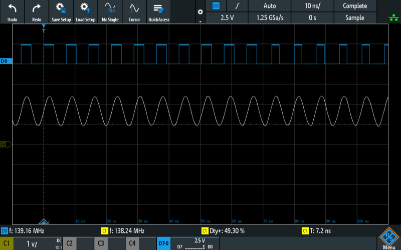
so now we have a 138MHz signal. Since the counter clock is 275MHz, the PWM output is at half of this.
Summary
This post should not be taken as GPIO toggling is a good thing, it usually is not. It is the best to use things like timers.
Although the processor clock is very high, and consequently various buses are also clocked at very high speeds, accessing a peripheral is very indirect. Every read or write transfer takes 2-3 cycles in a bus, and APB bus is not pipelined so there are wait states. So other than using timers, if you need something more than 10 MHz, I think it requires hardware support like various specialized peripherals like SPI. If you need to support something having both a high speed and a custom protocol, then there are not many options other than FPGAs.
Although the ideas in this post can be applied to other MCU series, the internal architecture will be different, so this will result different numbers in different series. Particularly, if the transfer controller (processor or DMA) is closer to the memory and to the peripheral, it may even work faster even if the processor is clocked at a lower frequency, since almost always the processor is not the bottleneck.
This work is licensed under a Creative Commons Attribution-NonCommercial-ShareAlike 4.0 International License.