AMD EPYC 7313P and Supermicro H12SSL NUMA Topology
I have recently installed an AMD EPYC 7313P CPU on a Supermicro H12SSL-NT mainboard. One thing special about EPYC processors is they are multi-chip CPUs, so a proper NUMA topology might make a difference in certain applications. This post is a brief summary.
Also, a practical point of this article is to show which PCIe slot belongs to which NUMA Domain on Supermicro H12SSL-NT. I have not seen this information anywhere, at least not directly.
There are two BIOS settings that affects NUMA Topology:
NUMA Nodes per Socket (NPS): sets memory access interleaving, and if ACPI SRAT L3 Cache as NUMA Domain is disabled, also defines the NUMA domains: NPS=1 means 1 domain per socket, NPS=2 means 2 domains per socket, NPS=4 means 4 domains per socket.ACPI SRAT L3 Cache as NUMA Domain: if enabled, L3 caches define the NUMA domains whereas NPS sets only the memory interleaving.
(please check AMD documents for more information about these settings)
AMD EPYC 7313P has a 4x4 configuration, meaning there are 4 Core/Cache Complex Dies (CCD). Each CCD has one Core Complex (CCX) which has 4 (physical) cores, and each core might run one or two threads. (Note: CCD and CCX is same for AMD EPYC 7003 Milan series, 1 CCD has only 1 CCX as opposed to 7002 Rome series)
Because of this, if I am not mistaken, enabling L3 Cache as NUMA Domain or disabling that but setting NPS=4 defines the same NUMA Domains (4 domains). So Enabling L3 Cache as NUMA Domain and setting NPS=4, is the same as setting only NPS=4 and disabling the other. (but enabling L3 Cache as NUMA Domain and setting NPS=1 is something different, even though the NUMA domains are same, memory interleaving is different)
When NPS=4 and L3 Cache as NUMA Domain is enabled (and SMT is enabled so each core runs 2 threads), NUMA topology is:
$ numactl -H

available: 4 nodes (0-3)
node 0 cpus: 0 1 2 3 16 17 18 19
node 0 size: 32015 MB
node 0 free: 29356 MB
node 1 cpus: 4 5 6 7 20 21 22 23
node 1 size: 32239 MB
node 1 free: 30103 MB
node 2 cpus: 8 9 10 11 24 25 26 27
node 2 size: 32239 MB
node 2 free: 30351 MB
node 3 cpus: 12 13 14 15 28 29 30 31
node 3 size: 32217 MB
node 3 free: 29519 MB
node distances:
node   0   1   2   3
  0:  10  12  12  12
  1:  12  10  12  12
  2:  12  12  10  12
  3:  12  12  12  10
or (the output below is edited to show only the cores and for clarity some lines are trimmed)
$ lstopo

Machine (126GB total) + Package L#0

  L3 L#0 (32MB)
    NUMANode L#0 (P#0 31GB)
    L2 L#0 (512KB)
      PU L#0 (P#0)
      PU L#1 (P#16)
    L2 L#1 (512KB)
      PU L#2 (P#1)
      PU L#3 (P#17)
    L2 L#2 (512KB)
      PU L#4 (P#2)
      PU L#5 (P#18)
    L2 L#3 (512KB)
      PU L#6 (P#3)
      PU L#7 (P#19)

  L3 L#1 (32MB)
    NUMANode L#1 (P#1 31GB)
    L2 L#4 (512KB)
      PU L#8 (P#4)
      PU L#9 (P#20)
    L2 L#5 (512KB)
      PU L#10 (P#5)
      PU L#11 (P#21)
    L2 L#6 (512KB)
      PU L#12 (P#6)
      PU L#13 (P#22)
    L2 L#7 (512KB)
      PU L#14 (P#7)
      PU L#15 (P#23)

  L3 L#2 (32MB)
    NUMANode L#2 (P#2 31GB)
    L2 L#8 (512KB)
      PU L#16 (P#8)
      PU L#17 (P#24)
    L2 L#9 (512KB)
      PU L#18 (P#9)
      PU L#19 (P#25)
    L2 L#10 (512KB)
      PU L#20 (P#10)
      PU L#21 (P#26)
    L2 L#11 (512KB)
      PU L#22 (P#11)
      PU L#23 (P#27)

  L3 L#3 (32MB)
    NUMANode L#3 (P#3 31GB)
    L2 L#12 (512KB)
      PU L#24 (P#12)
      PU L#25 (P#28)
    L2 L#13 (512KB)
      PU L#26 (P#13)
      PU L#27 (P#29)
    L2 L#14 (512KB)
      PU L#28 (P#14)
      PU L#29 (P#30)
    L2 L#15 (512KB)
      PU L#30 (P#15)
      PU L#31 (P#31)
So NUMA Node 0 is CCD 0 (or CCX 0) which contains 4 cores and each core contains two threads. So CCD 0/Core 0 has threads 0 and 16 which are shown as Core 0 and Core 16 in the operating system. As seen above, L3 is shared by all the cores in one CCD.
In addition to 4 CCDs, there is one I/O die (IOD) on the chip. IOD contains all 8 memory controllers, PCIe controllers (also 8 having x16 lanes) and some other things. The important thing is Memory controllers and PCIe controllers are also divided equally among all CCDs like L3 cache. The diagram below from AMD shows this nicely (open in new window for larger view):
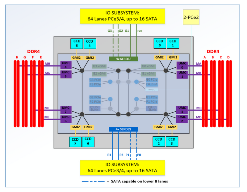
1P System Block Diagram (source: AMD PPR for AMD Family 19h
This diagram shows a CPU with 8 CCDs, but 7313P has only 4 CCDs, however it is still organized similarly (just assume there are only CCD 0, CCD 2, CCD 4 and CCD 6 on this diagram). So, as an example, CCD 0 has direct or more close/faster (than others) access to:
- Memory Controllers: UMC0 and UMC1 (MA and MB, 2 channels out of 8)
- PCIe Controllers: G0 and P0
Also, 4 out of 8 of x16 PCIe controllers (P0, P1, G2, G3) can be configured such that they function as x8 PCIe lanes and x8 SATA controllers.
(these do not mean that CCD0 cannot access G1, naturally all these are interconnected with so called AMD Infinity Fabric)
I have all 8 DIMMs populated so memory controllers are not that important but which PCIe slot belongs to which controllers ? H12SSL-NT manual has this diagram (again open in new window for a larger view):
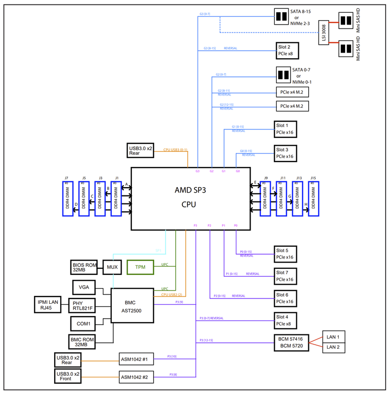
System Block Diagram (source: Supermicro H12SSL users manual
It does not mention which Slot or PCIe device is connected to which CCD, but the P0..3 and G0..3 indications in the diagram is as you guess the PCIe controllers. By looking at both diagrams, you can guess which Slots are in same or different CCDs.
So it should be (I number the CCDs from 0 to 3, it is not the same as the AMD’s diagram -because that one has 8 CCDs whereas I have 4-, but each of these CCDs are at one quadrant like in the diagram):
- CCD 0: P0, G0: Slot 5 x16, Slot 3 x16
- CCD 1: P1, G1: Slot 7 x16, Slot 1 x16
- CCD 2: P2, G2: Slot 6 x16, 2x M.2 (2x x4=x8), SATA0-7 (x8)
- CCD 3: P3, G3: Slot 4 x8, 2x ASM1042 USB (x2), AST2500 VGA (x1), BCM57416 (LAN) (x4). SATA8-15 (x8), Slot 2 x8
This can be verified by the operating system utilities (the output below is edited for clarity, I kept only I/0 parts not individual cores, I simplified I/O outputs and wrote actually at which Slot that device is installed and looking to the manual also the AMD CCD PCIe controller code Px or Gx):
$ lstopo

Machine (126GB total) + Package L#0
  L3 L#0 (32MB)
    NUMANode L#0 (P#0 31GB)

  L3 L#1 (32MB)
    NUMANode L#1 (P#1 31GB)
    HostBridge
      PCIBridge -- P1
        PCI 81:00.0 (VGA) - Slot 7 x16

  L3 L#2 (32MB)
    NUMANode L#2 (P#2 31GB)
    HostBridge
      PCIBridge -- G3
        PCI 41:00.0-3 (Ethernet) - Slot 2 x8
      PCIBridge -- P3
        PCI 42:00.0-3 (Ethernet) - Slot 4 x8
      PCIBridge -- P3
        PCIBridge
          PCI 45:00.0 (VGA)
      PCIBridge -- P3
        PCI 47:00.0 (Ethernet)
          Net "eno1np0"
        PCI 47:00.1 (Ethernet)
          Net "eno2np1"
      PCIBridge -- G2 (probably G2, if G3 then the one below is G2)
        PCI 4a:00.0 (SATA)
      PCIBridge -- G3
        PCI 4b:00.0 (SATA)

  L3 L#3 (32MB)
    NUMANode L#3 (P#3 31GB)
    HostBridge
      PCIBridge -- G2
        PCI 01:00.0 (NVMExp)
          Block(Disk) "nvme0n1"
      PCIBridge -- G2
        PCI 02:00.0 (NVMExp)
          Block(Disk) "nvme1n1"
I have cards installed only on Slot 7, Slot 4 and Slot 2. It seems:
- Node L#0 is CCD0, as it has no PCI devices attached.
- Node L#1 is CCD1, as it has Slot 7.
- Node L#2 is CCD2, since both Slot 2 and Slot 4 are there.
- Node L#3 is CCD3, since both M.2 devices are there.
But, you might have seen also, there is a problem. One of the SATA controllers (G2) is listed under node L#2 but this CCD should only have P3 and G3. So basically the SATA Controller on G2 should be listed under the other CCD/node L#3 together with M.2 devices at G2 as indicated by the manual. I do not know the reason for that yet. If I find the answer, I will update this post.
Update: I wrote my question above about the SATA controllers’ NUMA group to Supermicro, and being in touch with AMD, they confirmed that it is normal/expeted for G2 and G3 SATA controllers to be in the same NUMA group as they are under the same PCIe bus. So I think the diagrams I was showing is not enough or not telling the full story of the connections, IO SUBSYSTEM is not shown and it seems G2 and G3 are under the same PCIe root so under the same NUMA group.
(also a note, I actually installed a PCIe card to each Slot to check this information, and it is correct, the only problem is the SATA controller mentioned above)
So why is this information useful ? For example, if you want to use PCIe passthrough with a GPU or with a NIC (to use DPDK etc.), and if you configured the NUMA domains like above, you may want to pin the corresponding VM to the same NUMA domain where the PCIe card is connected. I have a GPU at Node L#1, so I will pin the corresponding VM to that domain, to Cores (as reported by the OS) 4,5,6,7,20,21,22,23. Does this matter ? Not sure, but it is the purpose of all these. You can also configure NPS=1 and disable L3 Cache as NUMA Domain, so you can have just one giant system with everthing in one NUMA Domain. (This works well for example on ESXi 7u2 and above since this version includes a EPYC aware scheduler, it automatically takes the actual CPU organization into account)
Also, as far as I understand, for example to use GPU Direct Storage, it is better to have GPU under the same PCIe root complex as NVMe devices. For this sytem, it means I should use Slot 6 for GPU.
This work is licensed under a Creative Commons Attribution-NonCommercial-ShareAlike 4.0 International License.