Measuring the Power Consumption of an ARM Cortex-M0 MCU: STM32F072
Introduction
This post is about power management, sleep modes and actual measured power consumption of an ARM Cortex-M0 processor. I will first give brief technical information regarding ARM Cortex-M0 and STM32F072 power management. Then, I will show the code examples and the current measurements.
The technical information in this post is a summary of important points from a few manuals and datasheets, but I explicitly state a few points that I find not clear enough in the documents. This can be helpful to some. The current measurements are, I think, still pretty rare to find on the internet as it required expensive equipment until recently.
Since the supply voltage, VDD, is fixed, the power consumption on the datasheets is given as current consumption values. Also, in this post, I will measure the current.
I will only show and measure sleep modes entered with WFI (wait for interrupt) instruction. I expect the results would be the same with WFE (wait for event).
One of the most popular articles in this blog is A Minimum Complete Tutorial of CPU Power Management, C-states and P-states. The power management on an embedded microcontroller is simpler, but it is on a different scale (uA) and also it can be easily measured. ARM Cortex-M0 does not have what is called P-states of a desktop CPU; it does not change its frequency and/or voltage while running. However, it can switch off various components of the microcontroller, similar to C-states of a desktop CPU.
Setup
I am using ST’s NUCLEO-F072RB development board, which has an STM32F072RB MCU.
For supplying power to the board and simultaneously measuring the current, I am using ST’s latest hardware tool STLINK-V3PWR. This is not only a debug probe (just as other STLINK tools) but also a basic (1-quadrant) source measure unit (SMU), which can supply 3.3V and measure the current up to 550mA at the same time at 50kHz bandwidth and 100kSPS sampling.
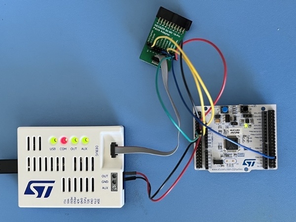
STLINK-V3PWR on the left, NUCLEO-F072RB on the right, and Segger Patch Adapter
There are two small issues with STLINK-V3PWR. First, it does not have an external power input. It takes all the power from USB-C data connection. Thus, it requires a USB data port that can supply >1.5A, so a charging port is required. This might be difficult to find in some computers and it is also difficult to find a USB hub with such ports (often the charging port is not a data port). I am using an Icy Box IB-HUB1405 USB hub with charging data ports providing up to 2.4A.
The second issue is the debug port connector. STLINK-V3PWR has a STDC14 connector and comes with three cables: STDC14 to STDC14, MIPI10 and MIPI20. However, most of the basic hardware development boards having an ARM Cortex M processor do not have MIPI10 connector but only exposed SWD interface pins. I have a Segger 50-Mil 10-Pin Patch Adapter, so I use this to take out the individual SWD signals from the debug port.
STLINK-V3PWR debug port is connected to Segger Patch Adapter with STDC14 to MIPI10 cable, and the following pins of MIPI10 are connected to NUCLEO board:
| MIPI10 Pin | NUCLEO-F072RB Pin |
|---|---|
| 1 VREF | CN7 12 (IOREF) |
| 2 SWDIO | CN7 13 (PA13) |
| 3 GND | CN7 20 (GND) |
| 4 SWCLK | CN7 15 (PA14) |
| 5 GND | |
| 6 SWO | CN10 31 (PB3) |
| 7 GND | |
| 8 N/C | |
| 9 GND | |
| 10 NRST | CN7 14 (RESET) |
The GND pins on MIPI10 are internally connected so only one (Pin 3) is connected to a GND (CN7 Pin 20) on the NUCLEO board.
IOREF is internally connected to +3.3V on the NUCLEO board, so it is used as VREF.
STLINK-V3PWR power output signal OUT is connected to CN7 Pin 16 (+3.3V), and the GND signal is connected to CN7 Pin 19 (GND).
In order to be able to supply an external +3.3V directly to CN7, either ST-LINK part of the board has to be removed or both SB2 (3.3V regulator) and SB12 (NRST) has to be removed. I already had a board with ST-LINK PCB cut off, so I started using that. However, I also removed SB2 to disconnect the 3.3V regulator. Because, I think, there is an internal reverse diode in the regulator and the LD3 (red) power led turns on even with external +3.3V. I did not want that as I do not know exactly how much current (a few mA) flows there. It would be impossible to measure uA level currents in deep sleep modes.
The STLINK-V3PWR output voltage is set to 3300mV.
I am using STM32CubeIDE and STM32CubeMonitor-Power on Windows.
STLINK-V3PWR vs. PPK2 (Power Profiler Kit II)
An alternative to STLINK-V3PWR is Nordic Semiconductor’s Power Profiler Kit II. They are priced approximately the same around 90 USD. I have purchased both from Farnell.
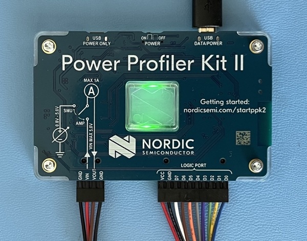
Power Profiler Kit II
The differences between the two are:
| Feature | STLINK-V3PWR | PPK2 (Power Profiler Kit II) |
|---|---|---|
| Measurement | Source Measure | Source Measure or Ampere Meter |
| Debug Probe | Yes | No |
| Extras | Bridges USB to SPI/I2C,CAN/GPIO | 8 channels logic analyzer |
| Power Input | USB, >1.5A needed | 2xUSB, one is power only |
| Measurement Range | 100nA to 550mA | 200nA to 1A |
| Measurement Accuracy | 2% | 20% (avg. current) |
| Voltage Output Range | 1.6V to 3.6V up to 550mA | 0.8V to 5V up to 1A |
| Measurement Bandwidth | 50 kHz | not mentioned |
| Sampling Rate | 100 kSPS | 100 kSPS |
The decision would be based on the following points:
- When >3.6V or >0.55A is needed, up to 5V and 1A, PPK2 is the only choice.
- There is no pure Ampere Meter in STLINK-V3PWR. It has to supply the power too.
- There is no debug port on PPK2. It is only for power measurement.
- I do not know maybe there is a mistake here but the measurement accuracy of STLINK-V3PWR is specified 10x better.
When 3.3V and less than 0.5A is needed, and particularly when working with ST MCUs, STLINK-V3PWR seems to be an obvious choice.
ARM Cortex-M0 Power Management
ARM Cortex-M0 has two sleep modes; SLEEP and DEEP SLEEP. In SLEEP mode, the processor clock is stopped. In DEEP SLEEP mode, the system clock is stopped, PLL and flash memory is switched off. Thus, basically, the peripherals are working in SLEEP, but switched off in DEEP SLEEP.
Entering sleep
There are two instructions that causes the processor to enter sleep modes; WFI (wait for interrupt) and WFE (wait for event). WFI directly puts the processor into sleep, whereas WFE works if event register contains 0. If event register is 1, WFE sets it to 0 and completes without entering to sleep mode.
SLEEPDEEP bit of the SCR (System Control Register) controls which sleep mode is entered.
There is an extra feature called sleep on exit. If SLEEPONEXIT bit of the SCR is set, the processor automatically enters into sleep after the execution of an exception handler (ISR) without returning to Thread mode. This is as if WFI is automatically called after the exception handler returns. This, for example, makes the processor respond only to interrupts and sleep in other times. As stacking and unstacking is unnecessary if only exception handlers are running, this further reduces the power consumption.
Waking up from WFI
When one of the following happens, sleep ends:
(these points are directly taken from the ARM Cortex-M0 devices generic user guide)
- an exception
- an interrupt becomes pending, which would preempt if PRIMASK was clear
- a Debug Entry request (even if debug is not enabled)
If PRIMASK register is not 0, it “prevents the activation of all exceptions with configurable priority”.
Waking up from WFE
When one of the following happens, sleep ends:
(these points are directly taken from the ARM Cortex-M0 devices generic user guide)
- an exception, unless masked by the exception mask registers or the current priority level
- an exception enters the Pending state, if
SEVONPENDbit in theSCRis set - a Debug Entry request, if debug is enabled
- an event signaled by a peripheral or another processor in a multiprocessor system using the
SEVinstruction
SEV instruction can also be used on a uniprocessor system, to send an event to itself.
Wakeup Interrupt Controller (WIC)
An ARM Cortex-M0 implementation may have an optional WIC, that can be used to wake the processor up from a deep sleep when an interrupt is detected.
An interrupt normally cannot wake the processor up from deep sleep, because NVIC is also not running. WIC is connected to power management unit, so when it detects an interrupt, it can generate a request for power and then NVIC can also function.
External event signal
An ARM Cortex-M0 implementation may have an external event signal to wake the processor up from a sleep initiated by WFE.
STM32F072 Power Management
STM32F072 is an ARM Cortex-M0 implementation. It implements both SLEEP and DEEP SLEEP modes. Furthermore, DEEP SLEEP is implemented in two different modes called STOP and STANDBY. Thus, it has four power states:
| State | Description |
|---|---|
| RUN | The normal operating state. |
| SLEEP | The processor clock is stopped, but the peripherals are working, including core system peripherals such as NVIC and SysTick. |
| STOP | All clocks in 1.8V domain is stopped. SRAM and registers are retained in order to be able to return back to RUN without losing the state. The 1.8V regulator can run in low power mode. |
| STANDBY | The 1.8V regulator is completely switched off, so entire 1.8V domain is powered off. As the state is not preserved, exiting STANDBY means a reset. |
After powering on and reset, the processor is in RUN mode. From RUN, it can go to SLEEP or STOP or STANDBY. From SLEEP and STOP, it can go back to RUN without losing the state. However, from STANDBY, it goes through reset before going to RUN mode again.
The SLEEPDEEP bit is used to distinguish SLEEP from STOP/STANDBY, but to distinguish STOP from STANDBY there is an additional PDDS bit of Power Control Register. There is also LPDS bit of the same register to select main or low power mode of the regulator in the STOP mode.
The diagram below is important for understanding the 1.8V domain. The processor and almost all the peripherals are in 1.8V domain as well as flash and SRAM memories. The sleep states work mostly on the 1.8V domain, so even if 1.8V domain is powered off, some other things can still be working. For example, VDDA domain contains the critical components of reset block and PLL, VDD domain contains standby circuitry and the voltage regulator supplying 1.8V, and the backup domain contains RTC (Real Time Clock). Because VDDA domain also contains ADC and DAC converters, and temperature sensor, these have to be handled separately before entering sleep mode. There is also a VDDIO2 domain, which can use a different voltage than VDD.
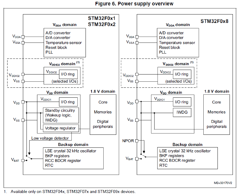
STM32F072B Power Supply Overview (source: RM0091)
A more detailed diagram showing exactly which peripheral is in which power domain is also available in the datasheet, DS9236.
As you can guess from the diagram, the clock source of RTC (in backup domain) and IWDG (in VDD domain) are never stopped, not even in STANDBY. They consume very less power, probably less than 1 uA.
As different parts of the MCU is powered down in low power states, different conditions should happen to exit from a particular low power state. This is summarized below:
| State | Exit by |
|---|---|
| SLEEP | any interrupt or event |
| STOP | EXTI, external interrupts specific communication peripherals |
| STANDBY | rising edge on WKUP pins RTC event |
STANDBY exit can also happen by external reset (NRST) and IWDG reset. I prefer to not list these above, because NRST and IWDG reset causes a reset from any state including RUN.
Based on above information, I believe, STM32F072 also contains the optional WIC, since it can wake up from DEEP SLEEP (STOP) with EXTI controller, which can “generate a wake-up request to the Power manager” (source: RM0091). NVIC works in SLEEP mode but not in STOP. So, without another component like WIC/EXTI, an interrupt cannot cause a wake-up.
Furthermore, on STM32F072, the 1.8V voltage regulator also has two modes; main and low power. In STOP mode, low power mode of the voltage regulator can be used to further decrease the consumption. In STANDBY mode, the regulator is effectively in zero power mode, it is completely switched off.
The deeper the processor sleeps, the more time it takes to wake up. It takes only 4 SYSCLK cycles to wake up from SLEEP (for 48MHz, less than 0.1us). In STOP mode, waking up from the low power mode of regulator takes more time, typically 2x more, e.g., 4.6us vs. 2.8us. From STANDBY mode, it typically takes 51us. Wake-up is faster for WFE, because the interrupt latency has to be added for WFI.
The power consumption in the specifications is indirectly given by $I_{DD}$, $I_{DDA}$ and power figures of peripherals in ${\mu}A/MHz$ units, since $V_{DD}$ is assumed to be fixed. $I_{DD}$ naturally includes the 1.8V domain as it is powered from $V_{DD}$. $I_{DD}$ also includes the backup domain when $V_{DD}$ is applied. $I_{DDA}$, on the other hand, is only for $V_{DDA}$ domain.
To give an idea, from the specification of STM32F072xB, when the processor is supplied with 3.3V (VDD), runs at 48 MHz with HSI48 clocksource with all the peripherals, VDDA monitoring (in STOP and STANDBY mode), and LSI and IWDG (in STANDBY mode) disabled, it typically consumes (all these values are from the datasheet):
13.1 mA + 322 uA = 13.4 mAin RUN mode.3.08 mA + 322 uA = 3.4 mAin SLEEP mode.15.8 uA + 1.5 uA = 17.3 uAin STOP mode with main regulator.3.6 uA + 1.5 uA = 5.1 uAin STOP mode with low power regulator.1.0 iA + 1.3 uA = 2.3 uAin STANDBY mode.
Above, the values on the left hand side are $I_{DD}$ and $I_{DDA}$. Please pay attention to the units. In RUN and SLEEP mode, the consumption is in mA range, whereas in STOP and STANDBY, it is in uA range, a 1000x difference.
The large difference in $I_{DDA}$ between RUN/SLEEP and STOP/STANDBY is due to HSI48, it typically consumes 312uA. On the other than, LSI, which can be enabled even in STANDBY, typically consumes 0.75uA.
Measurements
The experiments in this section are done with NUCLEO-F072RB board with two modifications as mentioned before. ST-LINK part is removed and the 3.3V regulator is disconnected by removing SB2.
On this board, both $V_{DDA}$ and $V_{DDIO2}$ are connected to $V_{DD}$, so what I am actually measuring is always the total current consumption of all the power domains. When comparing to specification, I always add $I_{DD}$ and $I_{DDA}$ and also make a rough estimate of the power consumption of the peripherals.
The two modifications leave only the LD2 (green) user led as an extra component that can consume power on the board other than the MCU. Almost all the peripherals of MCU are disabled, except:
- GPIO Port A, PA5 is connected to LD2 (green) User Led
- GPIO Port C, PC13 is connected to (blue) user button
- GPIO Port F, because of RCC_OSC_IN and RCC_OSC_OUT pins
- RTC
I use LD2 to see a change in the current consumption, and the user button to generate an interrupt for waking up the processor. EXTI line 4 to 15 interrupts are enabled.
RTC is activated on the IDE, and the RTC clock source is set to LSE. The wake-up timer is set in the code.
Important: There is a particular setting in the IDE, “Set all free pins as analog (to optimize the power consumption)”. Initially I thought this is maybe a too small difference but it is not. In deep sleep modes, the current consumption is in uA range, and actually if you do not enable this setting (or set all free pins as analog), the consumption is in mA range. I keep this setting enabled, if not stated otherwise. The analog configuration disables the output buffer, schmitt trigger and weak pull-up and pull-down resistors. It is the simplest GPIO configuration. Unfortunately, I think the power consumption is not specified based on the configuration, so I do not have any numbers.
HSI48 is used as the system clock source, and all prescalers are set to 1, thus the processor (and peripherals) runs at 48 MHz. Thus, PLL is disabled.
All measurements are done with 20kSPS sampling using STM32CubeMonitor-Power.
I compile all programs in Debug configuration, but I run without debugger attached as it would interfere with low power states.
Before looking at sleep states, I will show what happens in the special cases; power-on, reset and program download.
Power-On
Here is the current consumption during power-on:
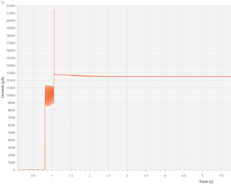
Current consumption during power-on
There is some activity at 10mA levels, then there is a transient going to 22mA, and then it settles (this is when the program starts to run) around 12.5mA. The program here is an empty while loop.
Reset
While the empty while loop program is running, I click reset target on CubeMonitor-Power, and this happens:
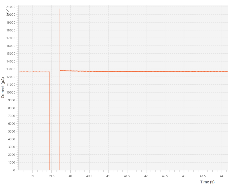
Current consumption during reset
There is no activity with a large variation as in power-on, but otherwise it is similar to power-on.
Program download
While the empty while loop program is running, I click “Run” on the IDE to initiate, I think, a reset, an erase, a download and a write, and then another reset:
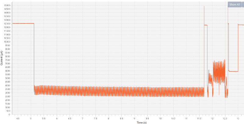
Current consumption during download
It takes some time at first, it takes around ~6 seconds consuming ~3mA. It is when IDE says waiting for debugger connection etc.
The program binary is ~13KB. This requires erasing 7 memory sectors (each page is 2KB). Page (2KB) erase time is specified as 20-40 ms. This should take 140-280ms and it should happen before write. The programming time is specified as 40-60us for 16-bits, so 20-30us/byte. 13KB would require ~250-400ms. So, basically write takes two times longer than erase.
Also, the specification says the write mode supply current is maximum 10mA, whereas the erase mode supply current is 12mA. Unfortunately, no minimum or typical values are given. Since it is given in mA levels, I guess the typical would be in mA levels as well.
I can only speculate this, but it looks like the section (between 11.75-12 seconds) at 5mA levels is erase, and the section (12-12.5 seconds) at 6mA levels is write.
Run
A simple program like the following, that toggles LD2 every second:
HAL_GPIO_WritePin(LD2_GPIO_Port, LD2_Pin, GPIO_PIN_RESET);
HAL_Delay(1000);
HAL_GPIO_WritePin(LD2_GPIO_Port, LD2_Pin, GPIO_PIN_SET);
HAL_Delay(1000);
results a current consumption like this:
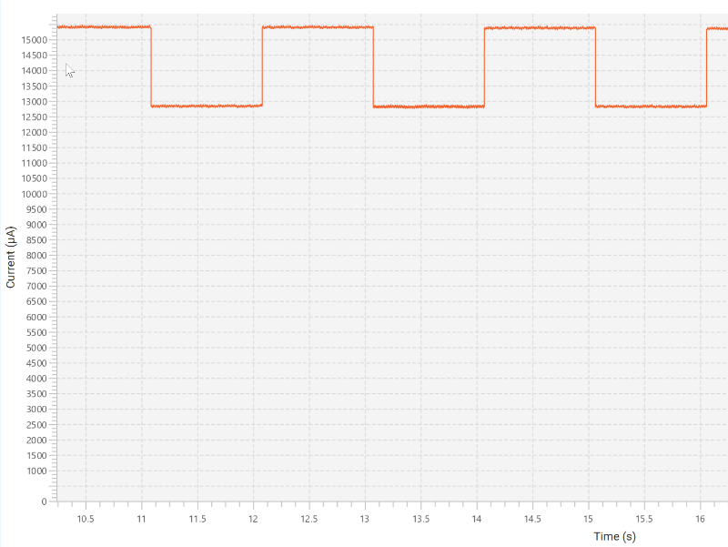
Current consumption at RUN mode at 48 MHz
It seems the LD2 led consumes ~2.5mA, and the MCU consumes almost 13mA. The specification indicates a typical consumption ~13.4mA, so this fits very well to the specification.
What happens if HSI is used as the system clock source, so the system and the processor clock is 8 MHz rather than 48 MHz ?
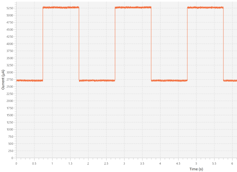
Current consumption at RUN mode at 8 MHz
The LD2 naturally still consumes ~2.5mA, but the MCU consumption decreased to 2.75mA from 13mA. This also very well matches to the typical specification value of approx. 3mA.
I set the system clock source back to HSI48, all the experiments below are done at 48 MHz as before.
Sleep
When testing the SLEEP mode, I changed the code slightly, now the LD2 is turned off for a second, turned on for a second, turned off for a second and then it goes to sleep.
HAL_GPIO_WritePin(LD2_GPIO_Port, LD2_Pin, GPIO_PIN_RESET);
HAL_Delay(1000);
HAL_GPIO_WritePin(LD2_GPIO_Port, LD2_Pin, GPIO_PIN_SET);
HAL_Delay(1000);
HAL_GPIO_WritePin(LD2_GPIO_Port, LD2_Pin, GPIO_PIN_RESET);
HAL_Delay(1000);

HAL_SuspendTick();
// PWR_MAINREGULATOR_ON is a dummy value here in STM32F0
HAL_PWR_EnterSLEEPMode(PWR_MAINREGULATOR_ON, PWR_SLEEPENTRY_WFI);
HAL_ResumeTick();
STM32F0 does not support changing the voltage regulator in sleep, so the first argument to HAL_PWR_EnterSLEEPMode is ignored.
The HAL_PWR_EnterSLEEPMode function is very simple. First, it clears the SLEEPDEEP bit of SCR, since this is not a deep sleep, and then calls WFI or WFE.
/* Clear SLEEPDEEP bit of Cortex System Control Register */
SCB->SCR &= (uint32_t)~((uint32_t)SCB_SCR_SLEEPDEEP_Msk);

/* Select SLEEP mode entry -------------------------------------------------*/
if(SLEEPEntry == PWR_SLEEPENTRY_WFI)
{
/* Request Wait For Interrupt */
    __WFI();
}
else
{
/* Request Wait For Event */
    __SEV();
__WFE();
__WFE();
}
__WFI, __WFE and __SEV are just placeholders for instructions, for example __WFI is defined (in CMSIS -Cortex Microcontroller Software Interface Standard-) as:
#define __WFI() __ASM volatile ("wfi")
I do not know for sure why rather than calling __WFE, it calls __SEV then __WFE and then the final __WFE, but probably, rather than doing:
// clear event register if set
if (event_register == 1) __WFE()
// sleep
__WFE()
it does:
// set event_register
__SEV
// clear event_register
__WEF
// sleep
__WEF
which is simpler than using a comparison and branch.
Also, before going to sleep, SysTick has to be suspended (it is not stopped in SLEEP mode). Because SysTick is a down-counter, and when it reaches 0, it generates an interrupt which would wake the processor up. HAL_SuspendTick() and HAL_ResumeTick() disables and enables SysTick interrupt. It is resumed when the processor is back from the sleep.
To wake up, I am using the user button which generates an interrupt.
Now, lets look at the current consumption.
Current consumption during SLEEP
During sleep mode, it consumes ~5.5mA. I think the specification value is ~3.5mA but this is without peripherals, so I think this still fits well to the specification. The peripherals consume less comparing the normal operating levels of the processor, but when the processor goes to low power modes, the amount peripherals contribute becomes important. For example, GPIOA consumes 8.2 uA/MHz, and Flash memory interface consumes 13 uA/Mhz, and for 48MHz, this makes ~1mA.
Stop
Now lets look at the deep sleep mode STOP. The code is similar to above but calling HAL_PWR_EnterSTOPMode and SystemClock_Config after wake-up:
HAL_GPIO_WritePin(LD2_GPIO_Port, LD2_Pin, GPIO_PIN_RESET);
HAL_Delay(1000);
HAL_GPIO_WritePin(LD2_GPIO_Port, LD2_Pin, GPIO_PIN_SET);
HAL_Delay(1000);
HAL_GPIO_WritePin(LD2_GPIO_Port, LD2_Pin, GPIO_PIN_RESET);
HAL_Delay(1000);

HAL_PWR_EnterSTOPMode(PWR_MAINREGULATOR_ON, PWR_STOPENTRY_WFI);
SystemClock_Config();
The HAL_PWR_EnterSTOPMode function is also simple:
/* Select the regulator state in STOP mode ---------------------------------*/
tmpreg = PWR->CR;

/* Clear PDDS and LPDS bits */
tmpreg &= (uint32_t)~(PWR_CR_PDDS | PWR_CR_LPDS);

/* Set LPDS bit according to Regulator value */
tmpreg |= Regulator;

/* Store the new value */
PWR->CR = tmpreg;

/* Set SLEEPDEEP bit of Cortex System Control Register */
SCB->SCR |= SCB_SCR_SLEEPDEEP_Msk;

/* Select STOP mode entry --------------------------------------------------*/
if(STOPEntry == PWR_STOPENTRY_WFI)
{
    /* Request Wait For Interrupt */
    __WFI();
}
else
{
    /* Request Wait For Event */
    __SEV();
    __WFE();
    __WFE();
}

/* Reset SLEEPDEEP bit of Cortex System Control Register */
SCB->SCR &= (uint32_t)~((uint32_t)SCB_SCR_SLEEPDEEP_Msk);
It first clears PDDS bit, and clears or sets LPDS depending on the regulator argument. Then sets the SLEEPDEEP bit and then calls __WFI or __WFE as before.
An important point regarding deep sleep is that, when exiting, the system clock source is set as HSI, so the clock configuration has to be redone, so I call SystemClock_Config above. Also, SysTick is already stopped in SLEEP mode, and it is resumed in SystemClock_Config after wake-up.
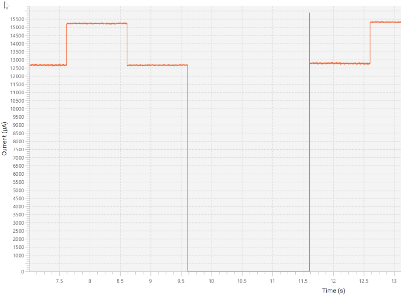
The program above results:
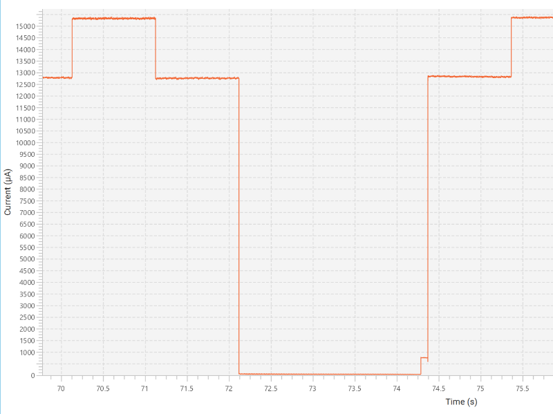
Current consumption when entering STOP mode with the main regulator
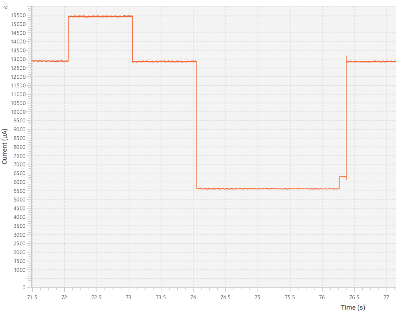
As a major difference here in STOP mode, comparing to SLEEP, the consumption goes to almost 0. The small increase less than 1mA (between 74-74.5s) is when I press the user button. Zooming in to STOP mode consumption:
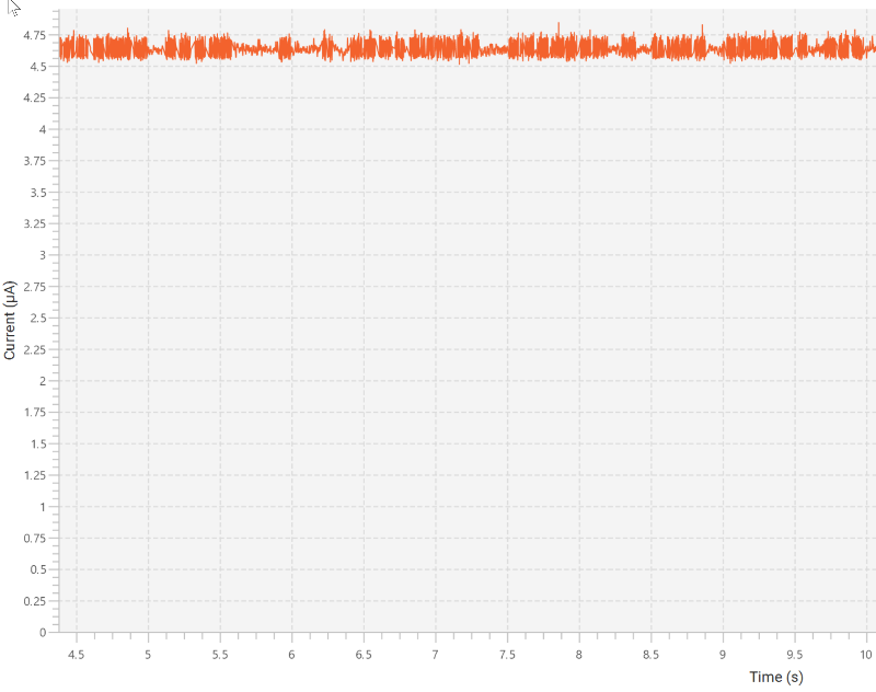
Current consumption of STOP mode with the main regulator
I think the midpoint is ~37.5uA. This is more than 100x decrease comparing to STOP mode.
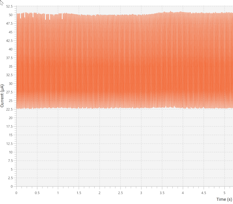
What about the low power regulator ? Here it is:
Current consumption of STOP mode with the low power regulator
Now the midpoint is ~25uA. It is a bit lower but not very different.
Both values are not far off from the values I mentioned before from the specification; however, at uA levels, the contribution of a small consumption of a peripheral might be relatively large.
Standby
I use the following code to test entering standby and measuring the current consumption. This time I set a wake-up timer to exit from the STANDBY mode.
RM0091 says for standby mode entry, WUF bit in Power Control/Status register has to be cleared, but this is not done by HAL_PWR_EnterSTANDBYMode, so a call to __HAL_PWR_CLEAR_FLAG is needed.
The timer configuration code sequence below is taken from STM32Cube_FW_F0_V1.11.0 example PWR_CurrentConsumption. It first disables all wake-up sources, then clears the related flags and the sets a wake-up timer to generate an interrupt.
HAL_GPIO_WritePin(LD2_GPIO_Port, LD2_Pin, GPIO_PIN_RESET);
HAL_Delay(1000);
HAL_GPIO_WritePin(LD2_GPIO_Port, LD2_Pin, GPIO_PIN_SET);
HAL_Delay(1000);
HAL_GPIO_WritePin(LD2_GPIO_Port, LD2_Pin, GPIO_PIN_RESET);
HAL_Delay(1000);

HAL_RTCEx_DeactivateWakeUpTimer(&hrtc);
__HAL_PWR_CLEAR_FLAG(PWR_FLAG_WU);
__HAL_RTC_WAKEUPTIMER_CLEAR_FLAG(&hrtc, RTC_FLAG_WUTF);
// LSE is 32.768Hz, 32768/16 is 2048
HAL_RTCEx_SetWakeUpTimer_IT(&hrtc, 2*2048, RTC_WAKEUPCLOCK_RTCCLK_DIV16);
HAL_PWR_EnterSTANDBYMode();
This results:
Current consumption when entering STANDBY
Similar to STOP mode, the consumption decreases to almost 0. However, one difference I recognize is the transient when waking up. This is similar to power-on or reset, I guess because this is a reset. Exit from STOP mode does not have this transient peak.
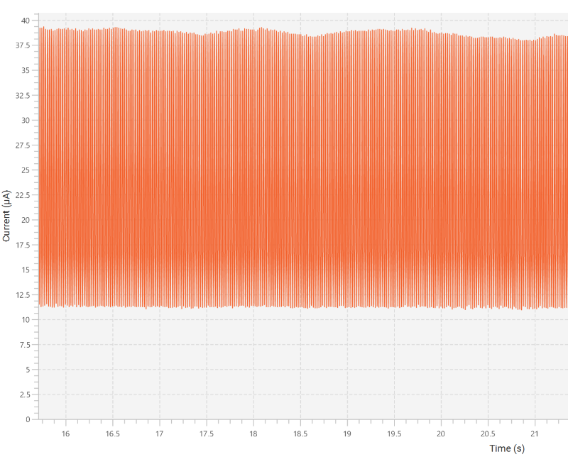
If I zoom to the uA levels during STANDBY mode:
Current consumption during STANDBY
It is 4.5uA, less than STOP mode as expected, but not hugely different.
Summary
To summarize what I learned writing this post:
- ARM Cortex-M0 has sleep and deep sleep modes.
- Deep sleep mode is implemented as STOP and STANDBY in STM32F072.
- The measured power consumption fits very well to the specification.
- There is not much difference between RUN and SLEEP in terms of power consumption. (<10x)
- There is a huge difference between RUN/SLEEP and STOP. (>100x)
- There is not much difference between STOP and STANDBY. (<10x)
- The difference between main regulator and low power regulator in STOP mode is small. (<10x)
- Setting the free pins as analog makes a difference, particularly in STOP mode.
- STLINK-V3PWR is a very nice gadget for analyzing the power consumption.
Resources
This work is licensed under a Creative Commons Attribution-NonCommercial-ShareAlike 4.0 International License.